Research Stories:

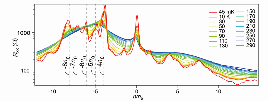
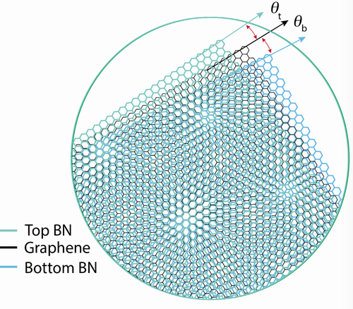
Moiré Superpotential.
h-BN/graphene/h-BN, with close to 0-degree alignment for both top and bottom surfaces, is found to show correlated insulating behavior at -5、-6、-7 n0 filling(i.e., each moiré unit cell is filled with 5、6、7 holes).
Click to read »

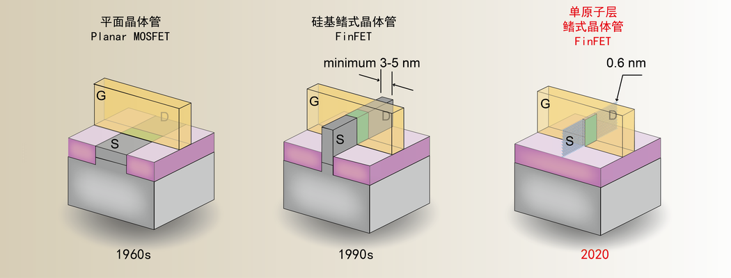
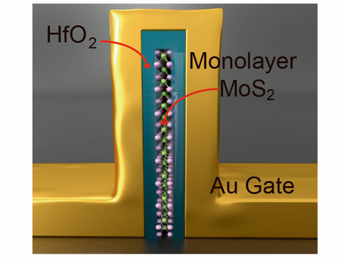
FinFET with 1 atom layer fin.
A templated growth method allows one to have vertically standing 2D materials with 300 nm height on a side wall of xoide. The width of fins in FinFETs can thus be shrinked down to sub-1 nm scale(0.6 nm).
Click to read »

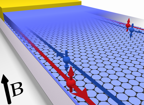
A robust QSHE in graphene/STO.
STO exhibits huge dielectric constat at low temperatures, and graphene very close to an STO substrate can manifest QSHE below 1T、above 100K, because of the screen of Coulomb interaction.
Click to read »

Gate tunbel Giant Anisotropic Resistance.
Few-layered GaTe is a 2D semiconductor with large in-plane anisotropic electrical conductivity, which is further gate tunable.
Click to read »

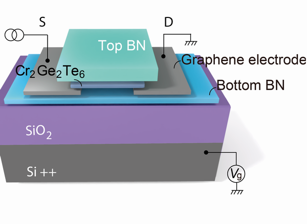
Spin-FET Built with 2D Material.
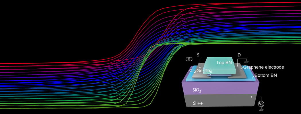
Few-layered Cr2Ge2Te6 is an intrinsic ferromagnetic semiconductor. Below its Curie temperature, a spin-FET is realized.
Click to read »

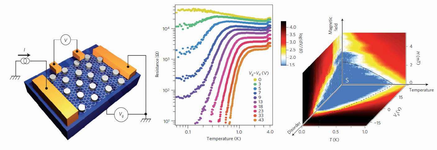
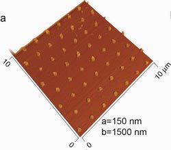
Gate Tunable Quantum Phase Transition.
When an array of superconducting islands is placed on graphene, the ground states can be shifted in between three states: superconductor, metal, and insulator.
Click to read »

Getting Rid of Multilayer Inhomogeneities.
A pulsed-growth method is invented to prevent the excessive carbon from precipitation and nucleating as multi-layer patches underneath the monolayer carpet.
Click to read »

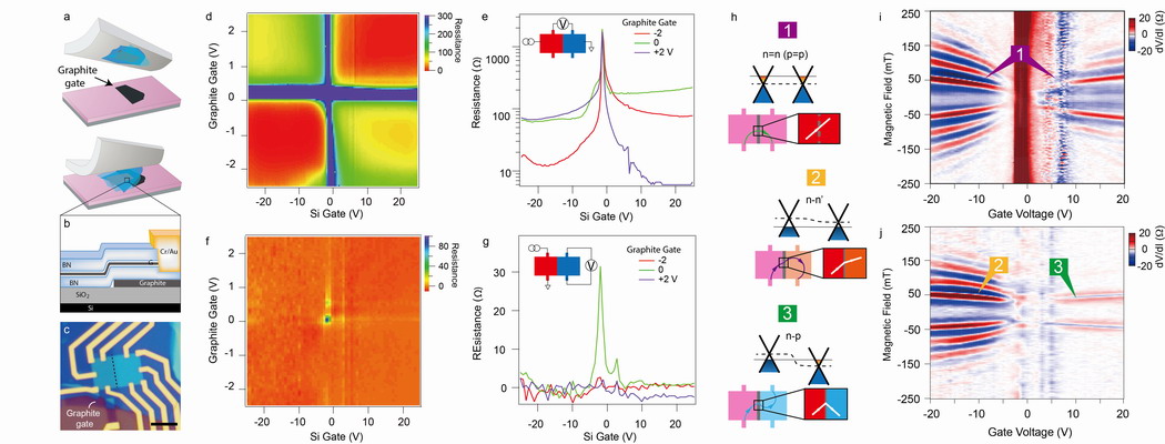
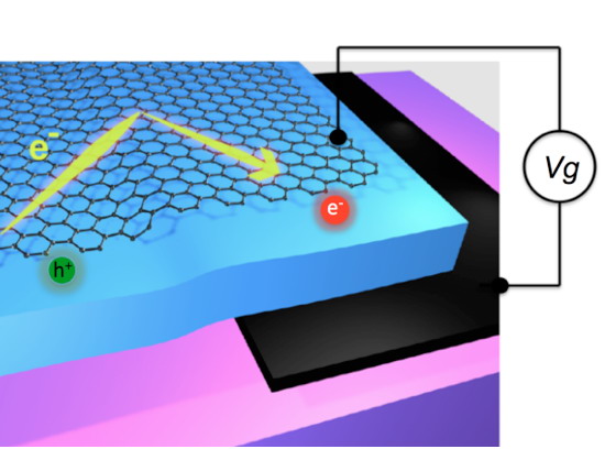
A ballistic pn junction in 2D.
By using atomically sharp gate, pn junction in a ballistic 2D electron gas is realized, thus forming a 2D Veselago lens.
Click to read »

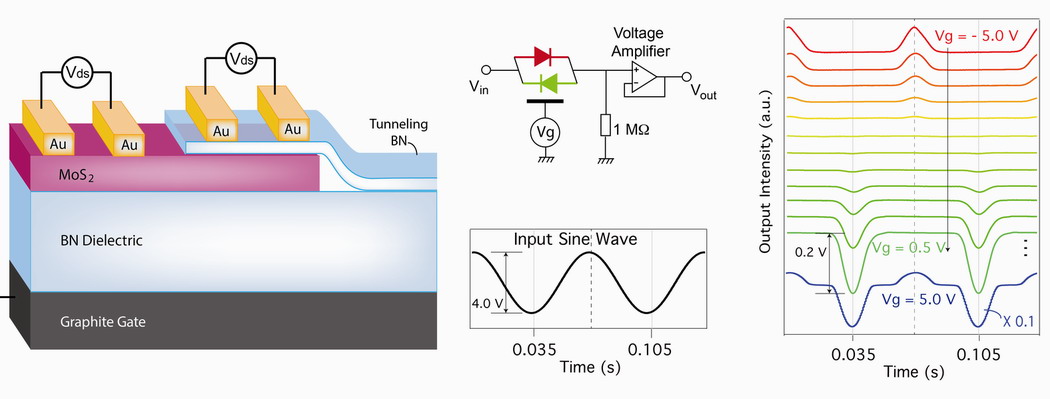
Polarity Tunable Diodes.
A tunnel-contacted MoS2 channel, can be programmed to show ‘pn’-‘Off’-‘np’-‘fullpass’ multi-functional behavior.
Click to read »
